Killing silicon: Inside IBM’s carbon nanotube computer chip lab
At IBM’s Watson Research Center in Yorktown Heights, New York, some of the world’s best physicists, chemists, and nanoengineers are trying to create the first high-density, self-assembling carbon nanotube computer chip process. In much the same way that Jack Kilby at Texas Instruments discovered the monolithic VLSI process for making silicon chips in 1958, IBM desperately wants to find the process that enables the creation of carbon nanotube chips.
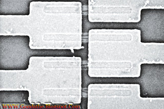
Metal pads, covering some carbon nanotubes
Progress is being made, however. Case in point: IBM has now managed to create a 10,000 carbon nanotube transistor chip, on top of a standard silicon wafer (pictured top). This is significant for two reasons. First, the process used is very similar to existing silicon chip fabrication processes — and when you’re talking about a trillion-dollar industry with stupendous amounts of capital investment in silicon tech, this is a very good thing. Second, IBM is reporting that its density of individually positioned carbon nanotubes is two orders of magnitude higher than any other research group’s efforts.
There’s still a lot of work to be done, though. The nanotube transistors are currently spaced 150nm apart, which is much farther than in silicon chips and will need to be reduced to reach the required feature density. The other problem is that the entire chip of 10,000 transistors currently only has one gate — the silicon wafer itself. Every transistor turns on and off at the same time. To fix this, the IBMers need to add electrodes to each of the carbon nanotubes — a step that also hinders graphene-based transistors. This is one of the key steps that IBM, and probably Intel and other silicon juggernauts, are currently working on.
Below are a few more pictures of IBM’s carbon nanotube computer chip, and the process behind its manufacture.
Carbon nanotubes are produced by burning carbon with an electric arc. About one quarter of the soot is nanotubes.
Carbon nanotubes are produced by burning carbon with an electric arc. About one quarter of the soot is nanotubes.
After the wafer is etched with trenches, it receives two liquid baths to deposit the carbon nanotubes
After the wafer is etched with trenches, it receives two liquid baths to deposit the carbon nanotubes
An IBMer, sliding the carbon nanotube transistor wafer into a testing machine
An IBMer, sliding the carbon nanotube transistor wafer into a testing machine
Black electrical probes, testing the carbon nanotube transistors
.jpg)
.jpg)
.jpg)
.jpg)
.jpg)
No comments:
Post a Comment